Scanning Tunneling Microscopy
Opening a New Era of Materials Engineering
In the last
decade, the ability of materials scientists to "nanoengineer" artificial
materials--to build materials atom by atom with a predetermined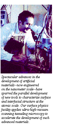 arrangement and goal--has enabled the development of new technologies with
applications that range from the spectacular to the mundane. For example,
x-ray mirrors composed of alternating, thin (less than 20-nanometer) films
of molybdenum and silicon constitute the optics that are used to
produce high-resolution pictures of the sun. Optoelectronic components
composed of alternating atomic layers of different elements are the
devices that enable us to extract information from video compact disks and
to generate and detect transoceanic telephone signals by fiberoptic
cables. The alternating, ultrathin layers of cobalt and iron in new
high-density magnetic storage heads, and increasingly miniature
microelectronics, are fundamental constituents of powerful desktop
computers, portable laptops, and pocket-size wireless telephones.
arrangement and goal--has enabled the development of new technologies with
applications that range from the spectacular to the mundane. For example,
x-ray mirrors composed of alternating, thin (less than 20-nanometer) films
of molybdenum and silicon constitute the optics that are used to
produce high-resolution pictures of the sun. Optoelectronic components
composed of alternating atomic layers of different elements are the
devices that enable us to extract information from video compact disks and
to generate and detect transoceanic telephone signals by fiberoptic
cables. The alternating, ultrathin layers of cobalt and iron in new
high-density magnetic storage heads, and increasingly miniature
microelectronics, are fundamental constituents of powerful desktop
computers, portable laptops, and pocket-size wireless telephones.
 The smaller these devices become, the
more their performance depends on the atomic ordering of their constituent
materials. Such details include the arrangement of atoms in crystal
structures and the presence, size, and density of grain boundaries,
impurities, dislocations, or other imperfections. Enhanced performance of
a device--increased reflectivity in the case of x-ray mirrors, efficiency
in the case of optoelectronics, switching speed in the case of transistors
for microelectronics, and hardness in the case of high-strength
coatings--therefore depends critically on the precise control of the
details of atomic ordering during manufacture. This is where LLNL's
surface physics facility in the Chemistry and Material Science Directorate
enters the picture with its ultra-high-vacuum scanning tunneling
microscopy capabilities. The smaller these devices become, the
more their performance depends on the atomic ordering of their constituent
materials. Such details include the arrangement of atoms in crystal
structures and the presence, size, and density of grain boundaries,
impurities, dislocations, or other imperfections. Enhanced performance of
a device--increased reflectivity in the case of x-ray mirrors, efficiency
in the case of optoelectronics, switching speed in the case of transistors
for microelectronics, and hardness in the case of high-strength
coatings--therefore depends critically on the precise control of the
details of atomic ordering during manufacture. This is where LLNL's
surface physics facility in the Chemistry and Material Science Directorate
enters the picture with its ultra-high-vacuum scanning tunneling
microscopy capabilities.
Analyzing
Atomic Arrangement
To diagnose the effect of atomic
arrangement on material performance, materials scientists use a battery of
techniques. Traditionally, diffraction-based probes have been the mainstay
of structural analysis, and have provided most of our basic knowledge
about the atomic arrangement of materials. In diffraction, a beam of light
or particles (neutrons, electrons, etc.) is scattered from an object, and
the three-dimensional, geometric distribution of the scattered rays is
determined by the structure of the object. For example, the pattern of
visible light reflected from the surface of an audio compact disc held
under bright light indicates the spacing of bits written onto the disc.
Similarly, the diffraction of beams of a wavelength that is comparable to
the spacing between atoms in a crystal indicates the spacing between the
atoms.
X-ray diffraction, the primary tool
for analyzing the long-range, atomic ordering of solids, enabled the
development of crystallography and provided the experimental data from
which the structure of DNA was deduced. Transmission electron microscopy,
another diffraction-based tool, is often used to provide images of
imperfections in crystals. In both x-ray diffraction and transmission
electron microscopy, however, diffraction measurements reveal the internal
atomic arrangements of a material only when crystalline order extends over
at least several hundred atomic spacings; in this case the material is
said to exhibit "long-range" order. In contrast, when crystalline order
exists over shorter distances, the material is said to exhibit
"short-range" order, which may not be detected by diffraction.
Analyzing
Surface Structure
These two diffraction techniques
present the "bulk," or three-dimensional, atomic arrangement of a
material. In nanoengineering, however, we must control how the individual
atomic layers of material are deposited. Because the structural integrity
of each atomic layer depends critically on the detailed atomic ordering of
the surface upon which it is deposited, we must be able to "see" the
atomic ordering, or structure, of that surface. To do this, we need a
separate class of diagnostics that presents the two-dimensional atomic
arrangement of the outermost layer of atoms in a material, rather than its
three-dimensional bulk structure.
Low-Energy
Electron Diffraction
For many years, the characterization
of surface structure has relied on the diffraction of electrons of low
energy (fewer than 200 V). Because such low-energy electrons do not
penetrate beyond a few atomic layers into a crystal, their diffraction
from a crystal yields the long-range atomic order on a surface. Although
low-energy electron diffraction is responsible for most of our current
knowledge of surface crystallography, it cannot reveal the short-range
crystalline order of nanometer-scale dimensions. Yet it is on this very
scale that clusters of deposited atoms initially aggregate, or nucleate,
and influence the atomic arrangement of subsequently grown material. In
this regime, true atomic resolution is necessary, and the scanning
tunneling microscope is indispensable.
Scanning
Tunneling Microscopy
The scanning tunneling microscope
(STM) provides a picture of the atomic arrangement of a surface by sensing
corrugations in the electron density of the surface that arise from the
positions of surface atoms (see Figure 1). A finely sharpened tungsten
wire (or "tip") is first positioned within 2 nanometers of the specimen by
a piezoelectric transducer, a ceramic positioning device that expands or
contracts in response to a change in applied voltage. This arrangement
enables us to control the motion of the tip with subnanometer precision.
At this small separation, as explained by the principles of quantum
mechanics, electrons "tunnel" through the gap, the region of vacuum
between the tip and the sample. If a small voltage (bias) is applied
between the tip and the sample, then a net current of electrons (the
"tunneling current") flows through the vacuum gap in the direction of the
bias. For a suitably sharpened tip--one that terminates ideally in a
single atom--the tunneling current is confined laterally to a radius of a
few tenths of a nanometer. The remarkable spatial resolution of the STM
derives from this lateral confinement of the current.
Next, additional piezoelectric
transducers are used to raster the tip across a small region of the
sample. As the tip scans the surface, corrugations in the electron density
at the surface of the sample cause corresponding variations in the
tunneling current. By detecting the very fine changes in tunneling current
as the tip is swept across the surface, we can derive a two-dimensional
map of the corrugations in electron density at the surface.
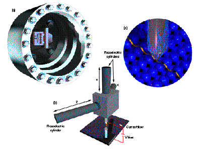 Figure 1. Artist's
renderings of a scanning tunneling microscope (STM). (a) Plan view of the
STM mounted in an ultra-high-vacuum chamber. (b) The probe tip as held by
a tripod, which consists of three piezoelectric cylinders that expand or
contract in the directions (x,y,z) shown to displace the tip. (c) A
close-up of the tip within tunneling distance of the surface of the
specimen being viewed, showing the ribbon-like path that the tip follows
above the surface atoms during scanning. Figure 1. Artist's
renderings of a scanning tunneling microscope (STM). (a) Plan view of the
STM mounted in an ultra-high-vacuum chamber. (b) The probe tip as held by
a tripod, which consists of three piezoelectric cylinders that expand or
contract in the directions (x,y,z) shown to displace the tip. (c) A
close-up of the tip within tunneling distance of the surface of the
specimen being viewed, showing the ribbon-like path that the tip follows
above the surface atoms during scanning.
Procedures for synthesizing various
nanoengineered materials often involve depositing the atoms onto a surface
in such a way that the surfaces remain free of contamination. The use of
ultra-high vacuum enables the preparation and atomic-resolution imaging of
atomically clean surfaces, which would otherwise be contaminated
immediately in air. That is why we integrated a scanning tunneling
microscope into an ultra-high-vacuum environment that includes facilities
for the preparation and maintenance of atomically clean surfaces, as well
as sources of the material to be deposited. We also integrated
complementary, conventional surface diagnostics equipment, such as a
low-energy electron diffraction probe, into this environment. The latter
measures the long-range order on a surface, and STM presents the
short-range order that otherwise might not be detected. In this
environment, the STM offers a new opportunity for direct diagnosis of how
the processing conditions affect the atomic details of surfaces.
How the
Molybdenum-Silicon Interface Forms
Recently, we used this combination of
surface diagnostics to study the structural development of thin films
(films from one atom to several tens of nanometers thick) resulting from
depositing molybdenum atoms on atomically clean silicon substrates. The
data from this study can be used to develop new processes for synthesizing
films that can achieve higher performance for particular applications.
For example, multilayer x-ray mirrors
composed of alternating, 5- to 20-nanometer-thick layers of molybdenum and
silicon achieve the best reflectivity when the interfaces between
molybdenum and silicon are most abrupt--that is, when pure molybdenum is
separated from pure silicon by a perfectly flat plane. However, molybdenum
and silicon tend to react to form crystalline compounds, or interfacial
silicides, which may adopt a variety of distinct crystal structures called
phases. Because these silicides degrade this interfacial abruptness, we
are trying to define processing conditions that minimize the amount of
interfacial silicide.
However, molybdenum silicides also
appear in other applications, such as high-temperature coatings and
diffusion barriers for interconnects in very large-scale integrated
circuits. For these applications, it may be desirable not to
minimize the amount of interfacial silicide but rather to maximize
the amount of a particular silicide phase, which may lead to enhanced
performance. Our analysis is therefore intended to provide a broad
correlation between the processing conditions (for example, substrate
temperature and deposition rate) and the microstructural details of the
resulting films, which ultimately determine how well the device will
perform for a specific application. We have found that film
morphology--characteristics such as roughness, crystalline structure, and
grain size and orientation--depends strongly on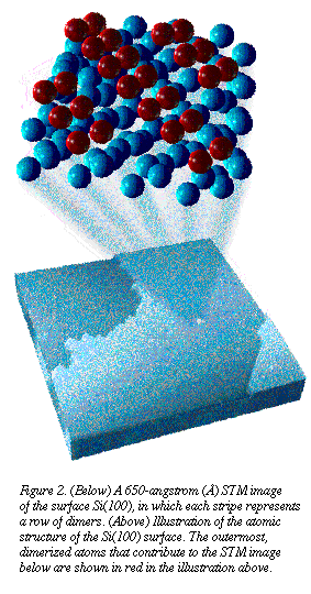 small structures called precursors. These structures form during the
initial stages of film growth and can only be detected with scanning
tunneling microscopy.
small structures called precursors. These structures form during the
initial stages of film growth and can only be detected with scanning
tunneling microscopy.
Phases and
Atomic Compositions
This reaction between molybdenum and
silicon exhibits a particularly rich variety of phases and relative
compositions of molybdenum and silicon, such as MoSi2 and Mo3Si.
The structure of disilicide thin films, as opposed to bulk crystals, is
further complicated by interfaces--both the silicide/substrate interface
and the silicide surface itself. For example, there is a thin disilicide
film phase that exhibits hexagonal symmetry that does not even appear in
the bulk phase. Furthermore, the precise temperature at which this phase
transforms to the equilibrium phase of tetragonal symmetry appears to be
highly process dependent. The STM can help us understand these phases and
transformations.
For example, we used the surface of
crystalline silicon--designated Si(100)--as the starting substrate for
film deposition. When clean Si(100) is exposed, the atoms of the surface
are rearranged--as is the case with most semiconductor materials. In fact,
bonds are formed between adjacent atoms, each pair of which is called a "dimer."
The dimers then align themselves into rows on the surface, as shown in
Figure 2. These surface structures are important to STM studies that seek
to extract chemical information about a particular surface.
Regimes of
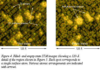
Silicide Film Growth
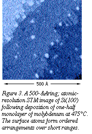
When we use STM to examine these
films, we find several regimes of silicide film growth. When molybdenum is
deposited on Si(100) at 475°C, a novel ordering of atoms occurs only
within the outermost layer of the surface (Figures 3 and 4). Because this
ordering cannot be detected by conventional x-ray crystallography and is
not readily detectable by electron diffraction, the resulting surface
previously was thought to be amorphous. With STM, it is now possible to
identify the presence and locally ordered character of this new
interfacial material.
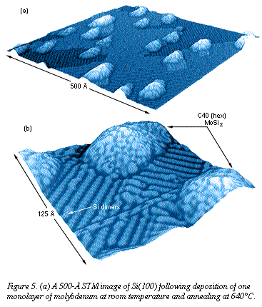
At higher temperatures (between 650
and 750°C) in this process, some of the material nucleates into the
hexagonal phase of disilicide MoSi2 (Figure 5). This nucleation
acts as a precursor for disilicide grains that grow when additional
molybdenum is deposited on the surface.
 The
third regime of disilicide growth occurs above 750°C. When molybdenum is
deposited at 770°C, tetragonal MoSi2 is formed. Figure 6, an
STM image of the resulting surface, displays plateaus with large, flat
terraces. Despite the variety of atomic arrangements observed in this
image, each superstructure suggests a simple relationship to the
periodicity (ordered, repeated atomic arrangement) of a specific face of
tetragonal MoSi2. The crystal face visible in the image then
specifies the orientation of growth of the specific grain, which is
preferentially oriented with respect to the silicon substrate. The
third regime of disilicide growth occurs above 750°C. When molybdenum is
deposited at 770°C, tetragonal MoSi2 is formed. Figure 6, an
STM image of the resulting surface, displays plateaus with large, flat
terraces. Despite the variety of atomic arrangements observed in this
image, each superstructure suggests a simple relationship to the
periodicity (ordered, repeated atomic arrangement) of a specific face of
tetragonal MoSi2. The crystal face visible in the image then
specifies the orientation of growth of the specific grain, which is
preferentially oriented with respect to the silicon substrate.
For example, the sets of small circles
in the three diagrams on the right-hand side of Figure 6 represent the
atomic arrangement of the [001] planes of tetragonal MoSi2. The large,
shaded circles represent atomic sites in a superstructure that would
correspond to the periodicity observed in the regions of the STM image. In
the diagram on the left-hand side, the small, white circles represent
silicon atoms in [100] planes, and the small, dark circles represent
molybdenum atoms in those planes. The large shaded circles then constitute
a superstructure that would correspond to the periodicity in the indicated
region of the image rotated approximately 37 deg with respect to the
neighboring regions. Such rotation would be required to achieve alignment
between a disilicide crystallite growing along its <100> axis and one
growing along its <001> axis. Both orientations of tetragonal MoSi2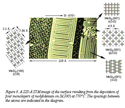 relative to the Si(100) substrate are consistent with those reported
previously for thicker disilicide films. Neither the existence of these
superstructures nor their relative prevalence was accessible from
measurements used in previous analyses of the molybdenum/silicon system.
relative to the Si(100) substrate are consistent with those reported
previously for thicker disilicide films. Neither the existence of these
superstructures nor their relative prevalence was accessible from
measurements used in previous analyses of the molybdenum/silicon system.
By associating specific
microstructures with the temperatures at which they are processed, we are
now equipped to determine the best procedure for synthesizing thin films
that have the microstructures necessary for particular applications. For
example, the temperature stability of multilayers used in x-ray mirrors is
known to be related strongly to the microstructure of the interfaces
between individual molybdenum and silicon layers. The deliberate promotion
during fabrication of one or another of the regimes of Mo/Si interfacial
structure that we have identified above may therefore lead to multilayers
with internal structure engineered for enhanced thermal stability.
With the advanced capabilities of STM,
the Laboratory can evaluate how processing parameters affect the atomic
structures of interfaces, identify surface defects that have a critical
influence on film growth, and control their occurrence, which will lead to
improved new materials with better performance characteristics.
Home
Research Area
Faculty staff students
Physics Resources
About us
|